Free Classifieds at AUNetAds.com - View Item Content by ID 2273764

Item ID 2273764 in Category: Computers - Hardware
Cannot view this item. It could be pending, expired or deleted.
Below item is randomly selected from the same category and may have similar content.
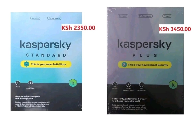
Brand new antivirus 00 | |
Brand new Antivirus Kaspersky 1 User Antivirus - 2350.00 Kaspersky 3 User devices internet Security - 3450.00 CONTACT : 0786 178372 or 0726 178372 LOCATION : Shop 501 (5th floor), Veteran House (Graffins college) Moi avenue, Nairobi Kenya.  | |
| Target State: All States Target City : All Cities Last Update : 08 November 2025 9:56 PM Number of Views: 185 | Item Owner : Moses xgamer Contact Email: (None) Contact Phone: (None) |
| Friendly reminder: Click here to read some tips. | |
© 2025 AUNetAds.com
USNetAds.com | GetJob.us | CANetAds.com | UKAdsList.com | INNetAds.com | CNNetAds.com | Hot-Web-Ads.com | USAOnlineClassifieds.com
2025-11-27 (0.848 sec)