Free Classifieds at AUNetAds.com - View Item Content by ID 2176836

AUNetAds > Business Opportunities > Other Business Ads > Item ID 2176836
Item ID 2176836 in Category: Business Opportunities - Other Business Ads
Cannot view this item. It could be pending, expired or deleted.
Below item is randomly selected from the same category and may have similar content.
Know About the SD Card Substrate Manufacturing Processes | |
The substrate material is prepared by cutting it into sheets of the required size. These sheets are then cleaned to remove any contaminants that could affect the manufacturing process or the performance of the final product. A thin layer of conductive material, such as copper, is then deposited onto the substrate using processes like electroplating or chemical vapor deposition (CVD). This copper layer is patterned using photolithography techniques to create the circuit traces that will connect the various components of the SD card. Contact info:- https://efpcb.wordpress.com/2024/04/24/know-about-the-sd-card-substrate-manufacturing-processes/ 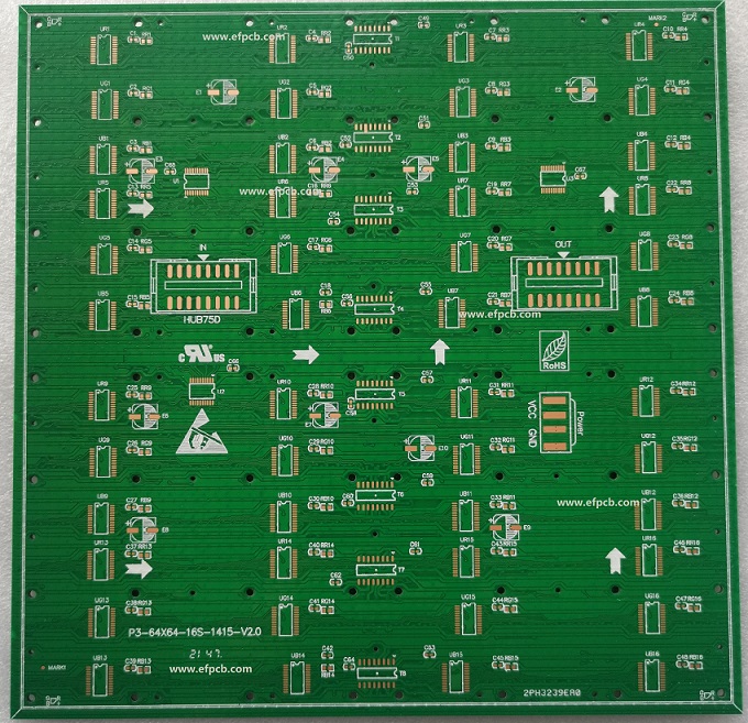 | |
| Related Link: Click here to visit item owner's website (0 hit) | |
| Target State: All States Target City : Guangdong Last Update : 04 May 2024 8:46 PM Number of Views: 36 | Item Owner : Shawn Wang Contact Email: Contact Phone: +86-755-23724206 |
| Friendly reminder: Click here to read some tips. | |
AUNetAds > Business Opportunities > Other Business Ads > Item ID 2176836
© 2024 AUNetAds.com
USNetAds.com | GetJob.us | CANetAds.com | UKAdsList.com | INNetAds.com | CNNetAds.com | Hot-Web-Ads.com | USAOnlineClassifieds.com
2024-05-05 (0.408 sec)